Consumer demand for electric vehicles (EVs) with a range comparable to internal combustion engines is currently outrunning the technology itself and, crucially, at a more accessible price point. More efficient drivetrains using semiconductor technologies such as Silicon Carbide (SiC) are enabling engineers to achieve the high voltage and power demands in a cost-effective way.
Electric cars are becoming more mainstream, with prices coming down and range going up. Sales of electric cars topped 2.1 million globally in 2019. According to the International Energy Agency’s report ‘Global EV Outlook 2020’, there were over 7.2 million electric passenger cars on the roads in 2019. However, continued growth depends on a number of factors. The reduced purchase subsidies in key markets has contributed to a significant drop in sales. There is also the COVID-19 pandemic to consider, which has had a major impact on car production globally this year. However, charging infrastructure improvements and consumer expectations of further technology improvements to lower vehicle prices and importantly, to give better range, remain key challenges.
More efficient drivetrains using semiconductor technologies such as Silicon Carbide (SiC) are enabling engineers to achieve the high voltage and power demands in a cost-effective way
Battery and motor manufacturers are reaching physical limits for performance using known technologies. However, in the drivetrain, where battery energy is converted into three-phase AC power for the motors, there is an obvious upgrade path away from traditional designs. This is to use wide band-gap semiconductors such as SiC.
Some EV applications have already started using SiC technology. These have largely been for low power applications, such as battery chargers, auxiliary DC-DC converters and solid-state circuit breakers. However, drivetrain power designers have been reluctant to use this technology, preferring to wait until it could achieve an acceptably low ON-resistance, better robustness and easier application. Now, a breakthrough in performance is addressing all of those concerns—the latest generation SiC-FET or ‘stacked cascode’ from UnitedSiC.
What is a stacked cascode?
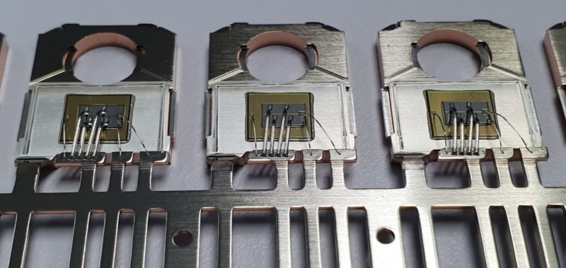
A stacked cascode is a device with two transistors stacked on top of one another: a high-voltage SiC JFET is connected in series with an optimised low voltage Si-MOSFET (see Figure 1). When the gate is high the MOSFET shorts the JFET gate-source, turning it ON. When the gate is low, the MOSFET drain voltage rises but only to the point that the JFET pinches OFF (ie the channel closes), which is around 10V. The result is a normally-OFF device with an easy gate drive. Moreover, it has all the benefits of a SiC device with low ON-resistance, high voltage and high-temperature operation, and an integral body diode effect with excellent reverse recovery characteristics.
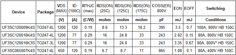
The cascode idea has been around for some time now but JFET versions are now achieving ON-resistances at high voltage ratings, making them close to the ‘ideal’ switch. Putting some figures to it, Table 1 is a selection of SiC-FETs from UnitedSiC showing RDS(ON) figures as low as 8.6 milliohms for a 1200V device and 6.7 Milliohms for a 650V device, both at 25 degrees Celsius. All devices are in the TO-247 package format, some with 4-lead Kelvin connections for optimum gate drive.
Low drain-source on resistance (RDS(ON)), output capacitance (COSS) and switching energy (EON and EOFF) values reduce conduction losses to a minimum. In addition, switches with inductive loads, such as in motor drives, have to ‘commutate’, that is, allow reverse conduction.
In IGBT circuits, a high-voltage parallel diode is necessary to allow reverse current flow. This is an extra cost and the diodes need to be high performance with minimal reverse recovery energy loss. SiC-MOSFETs, on the other hand, have an integral reverse diode but performance is relatively poor with a high forward voltage drop and significant recovery losses at operating temperatures. The SiC-FET, however, allows reverse conduction through the channel with no stored charge effects and low forward drop, effectively across the already low ON-resistance. The stacked Si-MOSFET in the package also conducts in reverse but being an optimised low voltage type, its body diode drop is small and also contributes little in recovery losses.
The latest generation SiC-FETs show lower losses than the traditional IGBT approach with additional side benefits. Table 2 shows calculated losses at six power levels comparing a current state-of-the-art IGBT module and parallel diode approach with SiC-FET versions.
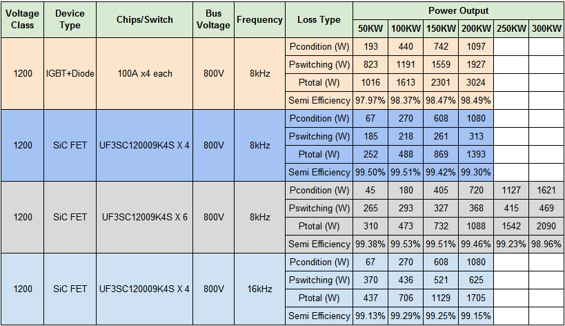
SiC-FETs consistently achieve nearly a four-fold reduction in power loss at the typical 50-100kW level and nearly three-fold reduction at 200kW. In EV applications, this equates to more energy available for extended range and reduced cooling requirements leading to smaller and lighter heatsinking, leading in turn to reduced load on the vehicle and better range—a virtuous circle. The availability of these low resistance devices in low cost discrete packages allow very economical inverter construction.
Although wide band-gap technology is relatively new, there have been understandable concerns about practical reliability. Latest generation SiC-FET parts now have extensive testing data and use mature production processes to guarantee robustness. They also have built-in advantages; apart from the inherent high-temperature capability of silicon carbide, SiC-FETs have a self-limiting avalanche drain voltage characteristic with the channel self-biasing to active mode with overvoltage, absorbing transient energy up to several joules.
Another SiC-FET benefit is that they are robust with short circuits. High current through the channel resistance produces a negative JFET gate bias, tending to switch the device OFF. Through self-heating, the positive temperature coefficient of the channel resistance then reduces the short circuit current further. This effect makes SiC-FETs easy to parallel with automatic current balancing, aided further by the relative insensitivity of the stacked MOSFET threshold voltage and reverse recovery characteristics to temperature changes.
EV charging
SiC-FETs are also ideal in fast charger applications where they offer peak efficiency in PFC front ends, and in the main DC-DC conversion stage—both typically using phase-shifted full bridge or LLC topologies. SiC diodes are already being used to implement output rectification in high voltage chargers due to their low drop and absence of reverse recovery losses. This is because synchronous rectification (SR) using Si-MOSFETs is complex at high voltage and can give no loss saving over diodes. However, using SiC-FETS with low RDS(ON) may prove more advantageous.
For example, at a 100A operating current with a 50% duty cycle, a SiC diode will have conduction losses of nearly 100W, but the UF3SC065007K4S will have conduction losses of just 45W. In addition, SR opens the possibility of bi-directional power flow, allowing the EV battery to return power to the grid for utility load-levelling for example, with corresponding financial benefits.
Solid state circuit breakers are an important application in EVs because isolating batteries during servicing and fault conditions is mandatory. With their normally ON characteristic, JFETs find a natural home here.
Backward compatibility
As UnitedSiC SiC-FETs are available in TO-247 three- and four-lead packages, they can be a drop-in replacement for many IGBTs and Si-MOSFETs in motor drives. This gives a significant boost in efficiency with little change in the circuit, apart from perhaps gate drive resistors and small snubbers to tailor the switching edges. Gate drive voltage requirements are non-critical, typically 0-12V. Other benefits such as reducing existing snubbers for lower loss and removing parallel diodes in designs that were originally IGBT-based could be considered. With the latest generation of low RDS(ON) devices from UnitedSiC, SiC-FETs are paving the way for the EV drivetrain revolution.
About the author: Anup Bhalla is Vice President of Engineering at UnitedSiC